Harvard Metamaterial Flat lens
July 4, 2016
After a first, unfortunate, experience in
elementary school with a
pinhole camera advertised on the back pages of a
comic book, I saved enough
money to buy a real
camera, a
35-mm film format rangefinder focusing camera, a
used Argus C3.
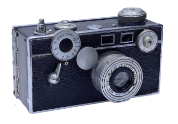
An Argus C3 camera.
I still have the lens from mine, although it's more of a keepsake than a useful item.
(Photo by Jarek Tuszynski, via Wikimedia Commons.)
In those days, long before the
Internet, the best way to learn about
technology was by subscribing to a
magazine on the subject. A side-benefit of having such a magazine was the interesting array of products advertised therein, with the affordable products located towards the back. These ads were an
education in themselves. The principal part of a camera is its
lens, and there was a plethora of articles and ads on lenses alone.
After a while, I purchased items to outfit a
home darkroom.
Photography in those days was a
chemical process, and it was interesting to me from that aspect, also. Not having enough money to buy a
commercial enlarger for my darkroom, I decided to build my own. I was happy to realize that the lens of my camera would work as an enlarger lens, but I needed to buy another type of lens, a
condenser lens.
Condenser lenses might be familiar to my readers who are
microscope users. Their purpose in an enlarger is to transform the
point source of
light from a
tungsten lamp to a wide,
parallel shaft of light. The parallel light passes through the
photographic negative, which is imaged onto
photographic paper by the exit lens. More light passes through the exit lens when another condenser lens is placed below the first.
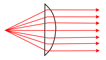
Ray diagram for a plano-convex condenser lens.
(Created using Inkscape.)
As I found, a condenser lens for this purpose was huge and heavy, since a lot of glass is needed to form parallel rays of light over a large
area (I designed the enlarger to accommodate
negatives up to
120-size, which were 60
mm x 60 mm). Over the years, high
refractive index were developed and the
processing of
optical materials has progressed to the point at which extremely small lenses of exceptional quality are now integrated into every
cellphone and
tablet computer.
The
technological battle cry of the last few
decades has been, "smaller is better," with
computer chips now containing
more than a billion transistors. While cellphone lenses are quite small, there are still applications for lenses that are even smaller. As one example, small, lightweight lenses are needed for
drones, some of which are the size of
flying insects. I wrote about one such drone in an
earlier article (Pop-Up Robots, February 23, 2012).
While a single large lens will
focus light, it's possible to combine many, smaller optical elements to do the same thing. The problem, however, is arranging these so that they act together and do not
distort the image.
Harvard University's Federico Capasso and
his research group have successfully made an extremely thin optical lens using an array of smaller optical elements.[1-3] The lens is made from a
computed array of high refractive index
titanium dioxide (
TiO2) pillars on a
silica glass (
SiO
2)
substrate (see figures).[1]
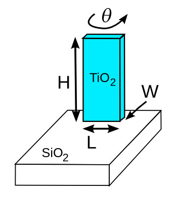
Process parameters for titania pillars on silica.
Since the length L is much greater than the width W, the phase shift of light through the lens at each point can be adjusted through rotation of the pillars.
(Created using Inkscape.)
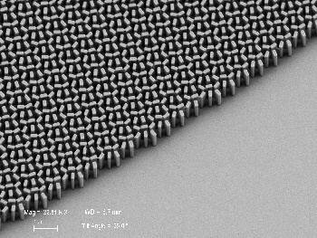
Scanning electron micrograph of the Harvard metamaterial lens. The titanium dioxide pillars are formed by atomic layer deposition (ALD) on a silica glass substrate. The scale bar is 2 millimeters.
(Capasso Lab image via Harvard University.)
The metalens, which is just 2 mm in dimension, has a
numerical aperture of 0.8, and it focuses light with
efficiencies as high as 86%.[1,3] The focusing was superb, being
diffraction-limited, but such a lens operates at just a particular
wavelength of light. It is out-of-focus at other wavelengths. However, such single wavelength lenses are useful for such things as
laser microscopy,
photolithography, and
spectroscopy.[1]
Once the technology of being able to build the phase-shifting titanium dioxide pillars is developed, the device
design is quite straightforward.
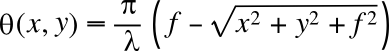
Geometrical optics provides a solution for the phase-shift at each region of the plate
(x,y) that's needed to focus a spot of light at a
focal length f for a wavelength
λ.[1]
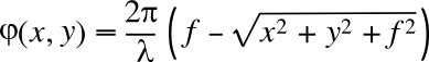
Since the length
L is much greater than the width
W, the phase shift of light through the length at each point can be adjusted through rotation of the pillars.[1]
Modern
computer technology allows an easy way to prepare a lithography mask of pillar elements that satisfies this equation.
Says Capasso, the senior
author of the
paper describing this lens,
"This technology is potentially revolutionary because it works in the visible spectrum, which means it has the capacity to replace lenses in all kinds of devices, from microscopes to cameras, to displays and cell phones... In the near future, metalenses will be manufactured/a> on a large scale at a small fraction of the cost of conventional lenses, using the foundries that mass produce microprocessors and memory chips."[2]
patent applications have been filed, and commercial opportunities are being explored.[2] This work was supported in part by the
Air Force Office of Scientific Research, the
Charles Stark Draper Laboratory, and
Thorlabs Inc.[1]
Fabrication was carried out in the
Harvard Center for Nanoscale Systems, which is supported by the
National Science Foundation.[1]
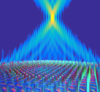
Artist's conception of metalens light focusing.
(Image: Peter Allen/Harvard John A. Paulson School of Engineering and Applied Sciences.)
![]()
References:
- Mohammadreza Khorasaninejad, Wei Ting Chen, Robert C. Devlin, Jaewon Oh, Alexander Y. Zhu, and Federico Capasso, "Metalenses at visible wavelengths: Diffraction-limited focusing and subwavelength resolution imaging," Science, vol. 352, no. 6290 (June 3, 2016), pp. 1190-1194, DOI: 10.1126/science.aaf6644.
- Leah Burrows, "Metalens works in the visible spectrum, sees smaller than a wavelength of light," Harvard University Press Release, June 2, 2016.
- Roland Pease, "Flat lens promises possible revolution in optics," BBC, June 3, 2016.
Permanent Link to this article
Linked Keywords: Elementary school; pinhole camera; advertising; advertised; comic book; money; camera; 35-mm film format; coincidence rangefinder; rangefinder focusing; used good; Argus C3; camera; lens; souvenir; keepsake; Jarek Tuszynsk; Wikimedia Commons; Internet; technology; magazine; education; home; darkroom; pPhotography; chemical process; commerce; commercial; enlarger; condenser lens; microscope; point source; light; tungsten lamp; parallel; photographic negative; photographic paper; ray; plano-convex; condenser lens; Inkscape; area; negative; 120 film; millimeter; mm; refractive index; processing; optics; optical; mobile phone; cellphone; tablet computer; technology; technological; battle cry; decade; integrated circuit; computer chip; transistor count; a billion transistors; unmanned aerial vehicle; drone; flying insect; focus; distortion; distort; Harvard School of Engineering and Applied Sciences; Harvard University; Federico Capasso; computation; compute; titanium dioxide; titanium; Ti; oxygen; O; fused quartz; silica glass; silicon; Si; substrate; process parameter; phase shift; light; rotation; Inkscape; scanning electron micrograph; metamaterial; atomic layer deposition; silica glass; millimeter; numerical aperture; efficiency; Gaussian beam; diffraction-limited; wavelength; laser microscopy; photolithography; spectroscopy; design; geometrical optics; focal length; computer; author; academic publishing; paper; visible spectrum; display; manufacturing; manufacture; semiconductor fabrication plant; foundry; mass production; microprocessor; dynamic random-access memory; memory chip; patent application; Air Force Office of Scientific Research; Charles Stark Draper Laboratory; Thorlabs Inc.; fabrication; Harvard Center for Nanoscale Systems; National Science Foundation; artist; Peter Allen.