| Tikalon Blog is now in archive mode.
An easily printed and saved version of this article, and a link
to a directory of all articles, can be found below: |
|
This article |
| Directory of all articles |
Graphene Transistors
October 21, 2010
Graphene is our current "wonder material." It's so important that only six years elapsed between its discovery and the award of a
Nobel Prize to its discovers, as I reviewed in a
previous article (2010 Nobel Prize in Physics, October 6, 2010). The pace of research from laboratory to practical application is usually long and arduous, but graphene has properties that mark it as a successor to
silicon and
other semiconductors for the fabrication of high speed, low power
integrated circuits. For this reason, there has been considerable research in transforming the exfoliated flecks of graphene stuck to
cellophane tape in the first experiments[1] into large areas on which many
transistors can be fabricated.
How do you make a graphene transistor?
IBM scientists showed an easy method in a paper published in
Science earlier this year.[2] They took a
silicon carbide wafer, one with a crystal orientation that exposed silicon planes at its face, and heated it above 1,000
oC to decompose the SiC to form a graphene layer at the surface. They covered the graphene with a 10 nm polymer layer (poly-hydroxy
styrene) and coated the polymer with an oxide to form a gate insulating layer for a metal top-gate
FET architecture. Metal source and drain electrodes were then deposited on the graphene with a channel of graphene between them, and a gate electrode was deposited in the channel. Although the gate length was a rather large 240 nm, the transistors had an upper operating frequency of 100 GHz. This performance exceeds that of the best silicon transistors of the same gate length.
Physicists and members of the
NSF-supported
Materials Research Science and Engineering Center at the
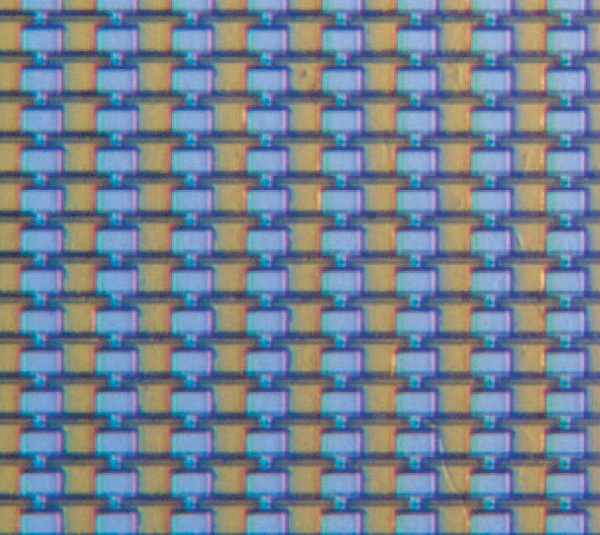
Georgia Institute of Technology have taken a different approach for producing graphene features on substrates that they call "templated growth."[3-6] They proved this technique by creating an array of 10,000 graphene transistors on a 0.24 square centimeter chip (see figure). The Georgia Tech team has produced nanoribbons as narrow as 40 nm by this technique.

Portion of an array of 10,000 graphene transistors fabricated by the templated growth technique (Georgia Tech Photo, from Ref. 5)
As you would suspect from the process name, they first etched patterns onto the silicon carbide surface before the
epitaxial growth of graphene. The graphene followed the template pattern to form nanoribbons of a controlled width without further processing, thereby keeping the graphene in pristine condition for subsequent fabrication steps. These graphene nanoribbons have smooth edges that avoid the electron-scattering effects that limit transistor performance. Just as in the IBM experiments, the transistors were top-gated.
The nanoribbon approach solves a fundamental problem in making graphene useful. Graphene is
semimetallic in patches larger than about a micrometer in dimension, and useful transistors can be made from graphene only if a
band gap is introduced. Nanoribbons do this by
quantum confinement, but only if the ribbon edges are smooth, something that the templated growth process accomplishes. The transistors exhibit an on-off ratio of 10 and
carrier mobility up to 2,700 cm
2 V
-1 s
-1 at room temperature.
The principle that large patches of graphene are conductors, while smaller patches are semiconductors, can be used to advantage in device fabrication.
Walter A. de Heer, Regents' Professor of Physics and leader of the Georgia Tech team says,[5]
"The same material can be either a conductor or a semiconductor depending on its shape... One of the major advantages of graphene electronics is to make the device leads and the semiconducting ribbons from the same material. That's important to avoid electrical resistance that builds up at junctions between different materials."
References:
- K. S. Novoselov, A. K. Geim, S. V. Morozov, D. Jiang, Y. Zhang, S. V. Dubonos, I. V. Grigorieva and A. A. Firsov, "Electric Field Effect in Atomically Thin Carbon Films," Science, vol. 306, no. 5696 (October 22, 2004), pp. 666-669.
- Y.-M. Lin, C. Dimitrakopoulos, K. A. Jenkins, D. B. Farmer, H.-Y. Chiu, A. Grill and Ph. Avouris, "100-GHz Transistors from Wafer-Scale Epitaxial Graphene," Science, vol. 327. no. 5966 (February 5, 2010), p. 662.
- John A. Rogers, "Nanoelectronics: Nanoribbons on the edge," Nature Nanotechnology vol. 5, no. 10, pp. 698-699 (published online October 6, 2010).
- M. Sprinkle, M. Ruan, Y. Hu, J. Hankinson, M. Rubio-Roy, B. Zhang, X. Wu, C. Berger and W. A. de Heer, "Scalable templated growth of graphene nanoribbons on SiC," Nature Nanotechnology vol. 5, no. 10, pp. 727-731 (published online October 3, 2010).
- John Toon, "Smoothing the Edges: New Graphene Fabrication Method Uses Silicon Carbide Templates to Create Desired Growth," Georgia Institute of Technology Press Release, October 5, 2010.
- Web Page of Walter de Heer's Epitaxial Graphene Lab.
Permanent Link to this article
Linked Keywords: Graphene; Nobel Prize; silicon; gallium arsenide; integrated circuits; cellophane; transistors; IBM; Science; silicon carbide; styrene; FET; National Science Foundation; NSF; Materials Research Science and Engineering Center; Georgia Institute of Technology; epitaxial growth; semimetallic; band gap; quantum confinement; carrier mobility; Walter A. de Heer.