Graphene-Copper Heat Sinks
March 26, 2014
Diamond has a very high
room temperature thermal conductivity,
22 W/(cm-K), which is five times greater than that of the excellent thermal conductor,
copper.[1] If you want to go to extremes, diamond formed exclusively from the
isotope 12C has a
theoretical thermal conductivity at 80
kelvin of about 2000 W/(cm-K).[2] Isotopic purity has this effect, since it reduces the scattering of
phonons, the carriers of
heat in
solids.
Diamond's high thermal conductivity is a consequence of its strong
covalent bonding which is efficient at coupling the
lattice vibrations responsible for heat transfer across large
volumes of a
crystal. This type of bonding is present, also, in the
carbon single layer sheets of
graphene, which has a thermal conductivity of about 50 W/(cm-K).[1]
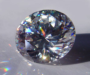
A cubic zirconia gemstone.
Cubic zirconia resembles diamond since it has a nearly identical refractive index, but it has a much smaller thermal conductivity.[3]
(Photo by Gregory Phillips, via Wikimedia Commons)
Diamond is sometimes used as a
heatsink material for high
power semiconductor devices, such as
power transistors and
laser diodes. This is now easier to do with the availability of
synthetic diamonds. Although the cost of diamond is high, the cost of the devices protected is often high enough to make the use of diamond
economical.
It would be useful to exploit the high thermal conductivity of graphene, but the problem here is that atomically thick graphene is generally placed on a
substrate, rather than being used as a substrate itself. A team of scientists from the
University of California, Riverside (Riverside, California), the
University of Manchester (Manchester, UK), and
Bluestone Global Tech (Wappingers Falls, New York) have overcome this limitation by demonstrating that deposition of graphene on copper increases copper's thermal conductivity.[4-5] Their results are reported in a recent issue of
Nano Letters.[4]
Deposition of graphene on copper is a surprisingly well developed
technology. A 2009 study demonstrated growth of
centimeter-sized patches of graphene on copper by
chemical vapor deposition using
methane.[6] In that study, most of the deposited area was single layer graphene with about 5% of the area being multiple layers. Since carbon has a low
solubility in copper, the process was self-limiting.[6]
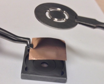
Since I'm an experimentalist, I enjoy images of how experiments are conducted.
Here, copper foil is being placed into a fixture prior to chemical vapor deposition of graphene.
(University of California, Riverside, image.)[5)]
In the experiments reported in Nano Letters, a single atomic layer of graphene was deposited by chemical vapor deposition on both sides of 9 μm thick copper foils. The resultant
composites showed an enhanced thermal conductivity at room temperature of up to 24%.[4-5] This was surprising, since the graphene added just two atomic layers to a copper substrate having thousands of atomic layers of copper.
As they found, it wasn't the graphene itself adding to the thermal conductivity, but a change in the
microstructure of the copper. The high
temperature chemical vapor deposition of graphene stimulated
grain growth in the copper foil (see figure). Larger grains lead to better thermal conductivity.[4-5] This effect was more pronounced for thinner copper foils, so there's the possibility for the formation of highly thermally conductive layers at the
nanometer level.[5]
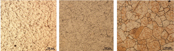
Photomicrographs of graphene layers on copper: Copper before thermal processing (left), copper after thermal processing (center), and copper after graphene deposition (right). The large copper grains are apparent. (University of California, Riverside, image.)[5)]
The research team plans to investigate graphene on nanometer thick copper substrates and develop a
theoretical model for the enhancement.[5] Says
Alexander A. Balandin,
Director of the UC-Riverside
Nano-Device Laboratory,
"This enhancement of copper's ability to conduct heat could become important in the development of hybrid copper — graphene interconnects for electronic chips that continue to get smaller and smaller."[5]
This research was funded by the
National Science Foundation, the
STARnet Center for Function Accelerated nanoMaterial Engineering, and the
Defense Advanced Research Projects Agency (DARPA).[5]
References:
- Wikipedia list of thermal conductivities.
- Lanhua Wei, P. K. Kuo, R. L. Thomas, T. R. Anthony and W. F. Banholzer, "Thermal conductivity of isotopically modified single crystal diamond," Physical Review Letters, vol. 70, no. 24 (June 14, 1993), pp. 3764-3767.
- Harder than Diamond, This Blog, August 31, 2012.
- Pradyumna Goli, Hao Ning, Xuesong Li, Ching Yu Lu, Konstantin S. Novoselov and Alexander A. Balandin, "Thermal Properties of Graphene–Copper–Graphene Heterogeneous Films," Nano Letters, vol. 14, no. 3 (March 12, 2014), pp. 1497-1503.
- Sean Nealon, "Creating a Graphene-Metal Sandwich to Improve Electronics," University of California, Riverside, Press Release, March 11, 2014.
- Xuesong Li, Weiwei Cai, Jinho An, Seyoung Kim, Junghyo Nah, Dongxing Yang, Richard Piner, Aruna Velamakanni, Inhwa Jung, Emanuel Tutuc, Sanjay K. Banerjee, Luigi Colombo and Rodney S. Ruoff, "Large-Area Synthesis of High-Quality and Uniform Graphene Films on Copper Foils," Science, vol. 324, no. 5932 (June 5, 2009), pp. 1312-1314.
Permanent Link to this article
Linked Keywords: Diamond; room temperature; thermal conductivity; copper; isotope of carbon; theory; theoretical; kelvin; phonon; heat; solid; covalent bond; crystal structure; lattice; atom vibration; volume; crystal; carbon; graphene; cubic zirconia; gemstone; refractive index; Wikimedia Commons; heatsink; material; electric power; semiconductor device; power transistor; laser diode; synthetic diamond; economics; economical; substrate; University of California, Riverside (Riverside, California); University of Manchester (Manchester, UK); Bluestone Global Tech (Wappingers Falls, New York); Nano Letters; technology; centimeter; chemical vapor deposition; methane; solid solution; solubility; experimentalist; experiment; composite material; composite; microstructure; temperature; grain growth; nanometer; photomicrograph; mathematical model; Alexander A. Balandin; Director; Nano-Device Laboratory; integrated circuit; electronic chip; National Science Foundation; STARnet Center for Function Accelerated nanoMaterial Engineering; DARPA; Defense Advanced Research Projects Agency.