Vacuum Transistor
May 23, 2012
A hybrid approach is often more effective than either of its parts.
Hybrid electric vehicles are one example of this, since they take advantage of the best properties of each component technology in its most
efficient regime. There's also the
peanut-butter-plus-chocolate paradigm that's now used in many
foodstuffs.
My first
electronic circuits, built during what is now called
middle school, were
vacuum tube circuits.
Guitar amplifiers were popular items at that same time, so I built several for my friends by harvesting parts from derelict
television sets.

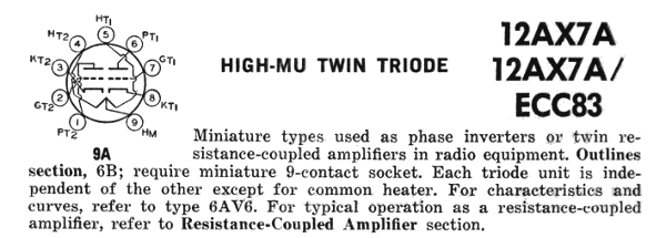
Portion of the section on the 12AX7 vacuum tube, from the 1966 edition of the RCA Receiving Tube Manual. (Scan of author's copy).[1)]
The first
transistors were low
gain devices, and they were unusual, since they were
current amplifiers, and not
transconductance amplifiers. The only way you could make a suitable
audio circuit using transistors was to use
step-up transformers between stages, which is one way to use current amplification to its best advantage. This low gain, and the low
frequency and
low power operation of transistors in the first two decades after they were introduced, are what kept vacuum tubes viable well into the 1960s.
The principal problems with vacuum tubes were their
cost of manufacture, their size, and their need for an internal
resistance heater to provide
thermionic emission of
electrons for operation. Transistors beat vacuum tubes on all counts, since they do not use thermionic emission, and they can be made very small.
Planar processing is an inexpensive manufacturing method when you divide the cost of the production facility between the millions, and later, billions, of transistors produced.
Vacuum tubes, even in later days, did have some advantages over transistors. At the time when the
electronics (also known as avionics) on western
military aircraft were becoming mostly solid state, the electronics in the
Soviet Mikoyan-Gurevich MiG-25 fighter aircraft were all vacuum tube. The vacuum tubes offered the advantage of being able to perform over a wide
temperature range; and they were resistant to
electromagnetic pulse (EMP). The MiG-25 was produced through 1984.

A head start on your video game design.
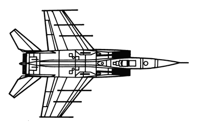
A drawing of the MIG-25, also known as the "Foxbat."
(Via Wikimedia Commons))
Naturally, one early idea was to miniaturize vacuum tubes.
RCA introduced its
nuvistor, a dime-sized vacuum tube, in 1959. The nuvistor was still a thermionic device, and it still required a heater. In 1973,
Charles Spindt and his colleagues at the
Stanford Research Institute (
Menlo Park, California) fabricated miniaturized vacuum tubes by a planar process.[2-3] These vacuum tubes solved two vacuum tube problems. They worked at a lower
voltage, and they didn't need a heater for thermionic emission.
The "Spindt"
cathodes generated electrons by
field emission, the idea that
electric fields are concentrated at sharp points. This idea was improved in a recent device that used
diamond as the field emitter.[4] Diamond works well in this application, since it has an extremely low
work function, so it will produce field emission electron beams at low voltage. I wrote about this device in a
previous article (Vacuum Tube Redux, August 9, 2011).
Although the Spindt device was used for
field emission displays, it has the fundamental problem that such vacuum tubes are difficult to produce with the
proper geometrical dimensions such as spacing between the tube elements. The alternative planar field emission architecture, the diamond device being an example, also has problems in definition of the area around the
gate, and the problem that some
current is drawn through the gate.
A different vacuum transistor has been designed by an international team of scientists from
NASA's Ames Research Center (Moffett Field, CA), and the
National Nanofab Center, Daejeon, Korea. This transistor, details of which are soon to be published in
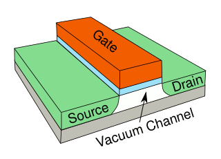
Applied Physics Letters,[5-6] uses a vertical architecture like the geometry of a standard
MOSFET to mitigate these problems (see figure). The device characteristics of this so-called "
vacuum channel transistor" are similar to those of a field effect transistor transistor.

Vacuum channel transistor architecture
(Drawing rendered by author using Inkscape)
Some previous vacuum channel architectures have been investigated using a buried gate[7] and complex vertical geometries.[8] The current design is simply fabricated using silicon planar processing techniques, and the spacing between the electron emitter and collector can be made to be smaller than the
lithography limit using a technique called
photoresist ashing. A resulting
nanoscale gap of 150 nm between the emitter and the collector allows operation at less than 10 volts. Devices functioned to 460
GHz, but operation into the
terahertz range is possible.[6]
Not only that, but a vacuum is not required. The channel dimension is less than the
mean free path of electrons in
air, and the low operating voltages are below the
ionization potential for
molecules in air.[6] High frequency operation is assured, since the
velocity of electrons in vacuum is 3 x 10
10 cm/
sec. The electron velocity in semiconductors is only as high as 5 x 10
7 cm/sec.
Acknowledgement:
Thanks to Jinwoo Han, and
Dr. Meyya Meyyappan, Director, the
Center for Nanotechnology,
NASA Ames Research Center, for providing me with an advance copy of the Applied Physics Letter paper.
References:
- 12AX7A, RCA Receiving Tube Manual, Radio Corporation of America, Electronic Components and Devices (Harrison, NJ, November, 1966), p. 389.
- C. A. Spindt, "A Thin‐Film Field‐Emission Cathode," Journal of Applied Physics, vol. 39, no. 7 (June 1, 1968), pp. 3504-3505.
- Charles A. Spindt, Kenneth R. Shouldersand Louis N. Heynick, "Field Emission Cathode Structures And Devices Utilizing Such Structures," US Patent No. 3,755,704, August 28, 1973.
- David Salisbury, "Designing diamond circuits for extreme environments," Vanderbilt University Press Release, Aug. 4, 2011.
- Jennifer Lauren Lee, "Return of the vacuum tube," American Institute of Physics Press Release, May 18, 2012.
- Jin-Woo Han, Jae Sub Oh and M. Meyyappan, "Vacuum nanoelectronics: back to the future? – gate insulated nanoscale vacuum channel transistor," to appear, Applied Physics Letters.
- Gyu Hyeong Cho, Ji Yeoul Ryoo, Myeoung Wun Hwang, Min Hyung Cho, Young Jin Woo and Young Ki Kim, "Vacuum Field Transistor," US Patent No. 6,437,360, August 20, 2002.
- Dae Yong Kim and Hyun Tak Kim, "Vacuum Channel Transistor and Manufacturing Method thereof," US Patent No. 8,159,119, April 17, 2012.
Permanent Link to this article
Linked Keywords: Hybrid electric vehicle; efficient energy use; Reese's Peanut Butter Cup; peanut-butter-plus-chocolate; paradigm; foodstuff; electronic circuit; middle school; vacuum tube; guitar amplifier; television set; 12AX7 vacuum tube; transistor; gain; current; amplifier; transconductance amplifier; audio; step-up transformer; frequency; low power; cost of manufacture; resistance heater; thermionic emission; electron; planar processing; electronics; military aircraft; Soviet Union; Mikoyan-Gurevich MiG-25; fighter aircraft; temperature; electromagnetic pulse; Wikimedia Commons; RCA; nuvistor; Charles Spindt; Stanford Research Institute; Menlo Park, California; voltage; cathode; field emission; electric field; diamond; work function; field emission display; design rule checking; proper geometrical dimension; gate; NASA Ames Research Center (Moffett Field, CA); National Nanofab Center, Daejeon, Korea; Applied Physics Letters; MOSFET; vacuum; Inkscape; photolithography; photoresist; nanoscale; GHz; mean free path; air; ionization potential; molecule; ballistic conduction; velocity; centimeter; cm; second; sec; Dr. Meyya Meyyappan; Center for Nanotechnology; NASA Ames Research Center; US Patent No. 3,755,704; US Patent No. 6,437,360; US Patent No. 8,159,119.