Transistors in Three Dimensions
May 10, 2011
As
urban developers have learned, when space is obtained at a premium, you build up, not out. The first
integrated circuits were
planar, with one device element being laid onto another. In the 1970s, a first attempt was made to transcend this
two-dimensionality by etching V-shaped grooves in
silicon wafers.
This
vertical metal oxide semiconductor, or VMOS, structure allows a greater current-handling capability.
Crystallography is an enabler for this process, since
etching a
(100) silicon surface will produce the grooves by exposing
(111) crystal planes that are at an angle of 54.74° with the (100) surface.
Potassium hydroxide is the usual etchant.
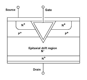
The VMOS transistor structure. The grooves are (111) planes of silicon exposed by etching of the (100) wafer surface.
(Via Wikimedia Commons)
Although there are grooves in the VMOS architecture, everything is backfilled, and it looks like a planer device. I still think it qualifies as the first three-dimensional
transistor architecture, and I'm sure that its inventors thought that it was an extremely unique and ambitious approach.
In 2002, thirty years after VMOS,
Intel Corporation produced its first examples of a different type of three dimensional
field effect transistor (FET), called tri-gate. Now, Intel has announced that it has commercialized this advance in field effect transistor technology that took the idea of building structures in the vertical dimension to new heights (pun intended). Not pulling any punches, Intel is producing these transistors with the extremely small gate width of 22
nm.[1-5]
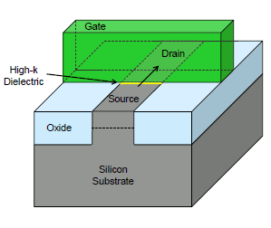
Clockwise from upper left, a planar transistor, a single-fin tri-gate transistor, and a multi-fin tri-gate transistor.
(Intel Corp, Ref. 5)
Intel's tri-gate architecture produces FETs that operate at lower
voltage and have lower
leakage, properties that make them useful for mobile computing devices. These 22 nm tri-gate transistors have up to a 37 percent performance increase over the 32 nm planar transistors of Intel's previous process. In a tri-gate FET, the gate covers three surfaces of a silicon fin, as seen in the figures. This allows an FET "on" state with lower resistance, and an FET "off" state with high isolation.
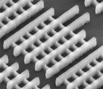
Yes, it's real.
Micrograph of multi-fin tri-gate FETs.
(Intel Corp., Ref. 5)
Intel co-founder,
Gordon E. Moore of the eponymous
Moore's Law, had this to say about the tri-gate process:[6]
"For years we have seen limits to how small transistors can get... This change in the basic structure is a truly revolutionary approach, and one that should allow Moore's Law, and the historic pace of innovation, to continue."
Now for my idea of a more energy-efficient transistor architecture. My Fourtran architecture (not to be confused with
Fortran), is a
four-dimensional approach that has transistors appear only when needed, and disappear when they are no longer in use. Best transistor architecture, ever!
References:
- Art Wittmann, "Intel Makes 3-D Transistors Reality," InformationWeek, May 4, 2011.
- Intel Reinvents Transistors Using New 3-D Structure, Intel Press Release, May 4, 2011.
- Robert S. Chau, "Integrated CMOS Tri-Gate Transistors Paving the Way to Future Technology Generations," Intel Web Site.
- Robert S. Chau, et al., "Tri-Gate Transistor Architecture with High-k Gate Dielectrics, Metal Gates and Strain Engineering," VLSI Conference, June, 2006, Conference, via Intel Web Site.
- Mark Bohr and Kaizad Mistry, "Intel’s Revolutionary 22 nm Transistor Technology," Intel Web Site, May, 2011.
- Jeff Bruner, "Intel 22nm 3-D Tri-Gate Transistor Technology," Intel Web Site, May 2, 2011.
Permanent Link to this article
Linked Keywords: Urban_planning; urban developer; integrated circuits; planar; two-dimensionality; silicon; wafers; vertical metal oxide semiconductor; crystallography; etching; Miller index; (100); (111); potassium hydroxide; Wikimedia Commons; transistor; Intel Corporation; field effect transistor; nanometer; nm; voltage; leakage; Gordon E. Moore; Moore's Law; Fortran; four-dimensional space.