Reaching the Bottom
May 3, 2011
Everyone is familiar with
Richard Feynman's December 29, 1959, talk, "
There's Plenty of Room at the Bottom." As we have found, there's a lot of playing field at the
nanoscale. Thirty years ago I was working with
magnetic bubbles devices with three
micrometer (3000
nm) features. After a few years, we had pushed this scale to 800
nanometers. Now,
integrated circuits are routinely made using 100 nm
design rules.

Feynman on the nanoscale.
This very small version of Richard Feynman's Los Alamos National Laboratory ID badge photograph is the largest clear public domain image available on the Internet.
(US Government photograph, via Wikimedia Commons).
Aside from the practical difficulty in producing multiple instances of smaller and smaller features, is there any intrinsic limit as to how small a nanoscale device can be? After all,
materials are made from
atoms, and the properties of a small clump of atoms are not the same as those of a larger chunk. The question of how small we can actually go - where the "bottom" really exists - is one that
Michael Kelly of the
Cambridge University Centre for Advanced Photonics and Electronics asks in a recent paper in the journal,
Nanotechnology.[1-2]
There are two methods available for production of a nanoscale device. The subtractive process, which Kelly calls the "top-down" manufacturing approach, involves the traditional
semiconductor processing step of
etching a
substrate. The additive, or bottom-up approach, involves pick-and-place of useful elements onto a substrate. A tour de force example of the bottom-up approach is the use of an
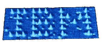
atomic force microscope to arrange atoms into a corporate logo. Kelly sees top-down as the only viable method for production of commercial nanoscale devices.
Kelly sees two limits in top-down manufacturing. The first is a 3 nm limit on creation of one-off structures. There are about fifty
silicon atoms per cubic nanometer, so this 3 nm limit corresponds to a little more than a thousand atoms. Since most useful nanomaterials are
binary compounds (e.g.,
ZnO) this would be just a few hundred functional units, not all of which would be in the
bulk crystal and exhibit the bulk crystal properties.

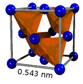
A silicon unit cell with silicon tetrahedra emphasized.
There are eight silicon atoms per unit cell.
(Image by Pieter Kuiper, via Wikimedia Commons).
Kelly's second limit is 7 nm, or about 17,000 silicon atoms. This is the limit that he sees in manufacturing nano-sized arrays of acceptable yield to a particular device specification. It's not difficult to see why this would be true. The
lattice constant of
silicon is 543 pm, or about half a nanometer. When you're forming silicon patches of 7 nm size, one
unit cell plane is about 8% of this dimension.
A good model system is an array of vertical pillars, and Kelly does a
statistical analysis of such arrays that confirms our premonitions in the preceding paragraphs.
In summary, Kelly has a caveat for the nanotechnology community:
"If more work is devoted to the hard problem of understanding just what can be manufactured and how, at the expense of more studies of things that cannot be manufactured under the conditions of the present theorem, then that too is good for science and for technology."[2]

Obligatory "bottom-up" nanoscale photograph.
The IBM logo rendered with xenon atoms in 1990.
(Via IBM).
References:
- M J Kelly, "Intrinsic top-down unmanufacturability," Nanotechnology, vol. 22 no. 24, April 21, 2011
- Joe Winters, "Limit to nanotechnology mass-production?" Institute of Physics Press Release, April 21, 2011
- IBM web site images, terms and conditions.
Permanent Link to this article
Linked Keywords: Richard Feynman; There's Plenty of Room at the Bottom; nanoscopic scale; magnetic bubbles devices; micrometer; nm; nanometer;integrated circuit; design rule; Wikimedia Commons; materials; atom; Michael Kelly; Cambridge University; Centre for Advanced Photonics and Electronics; Nanotechnology; semiconductor; etching; substrate; atomic force microscope; silicon; binary compound; ZnO; crystal; Pieter Kuiper; lattice constant; silicon; unit cell; statistical analysis; IBM.