Vacuum Transistors
July 11, 2014 Stating the obvious, electronic materials have the limitation that they're composed of matter. In that sense they're subject to material limitations, such as electrical conductivity when it isn't desired, and speed-limiting permittivity. As its name implies, permittivity is a measure of how a material will permit passage of an electric field. Material limitations are the reason for a revival of interest in vacuum electronic devices. I've written two previous articles on this topic, Vacuum Tube Redux (August 9, 2011), and Vacuum Transistor (May 23, 2012). The first vacuum electronic device was the vacuum tube, a component that defined electronics through the 1950s. One indication of both the ubiquity and the lack of reliability of vacuum tubes was the presence of vacuum tube testers at the corner drug store. You could test the vacuum tubes from your television, radio, and record player, there, and buy replacements. Vacuum tubes had a few advantages over early transistors. They were operable over a wider frequency range and at higher power. In the first few decades after the invention of the transistor, it wasn't possible to have a transistorized FM radio, or a transistorized guitar amplifier. As transistors increased in quality and declined in cost, vacuum tube technology was abandoned. There was an attempt by RCA to miniaturize vacuum tubes, but its nuvistor needed a heated cathode to generate an electron beam by thermionic emission. Thermionic emission isn't the only way to generate electrons. The large electric field at the tip of a pointed conductor will produce electrons by field electron emission. In theory, the electric field there is infinity, which would definitely remove electrons from a conductor. In practice, the electric field, as defined by the Fowler–Nordheim equations, is large, but less. The importance of these equations by British physicist, Ralph H. Fowler and German-American physicist, Lothar Nordheim was underscored to me by the phenomenal number of times they were mentioned by the professor of one of my graduate courses. In the 1970s, Charles Spindt and his colleagues at the Stanford Research Institute (Menlo Park, California) fabricated miniaturized field emission vacuum tubes by the same planar processing techniques used for integrated circuits.[1-2] These devices, as illustrated in the figure, also worked at a lower voltage than thermionic vacuum tubes because of their small dimension.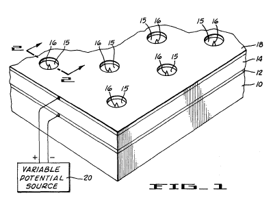 | Fig. 1 of US Patent No. 3,755,704, "Field Emission Cathode Structures And Devices Utilizing Such Structures," by Charles A. Spindt, Kenneth R. Shouldersand Louis N. Heynick, August 28, 1973. (Via Google Patents).[2] |
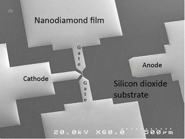
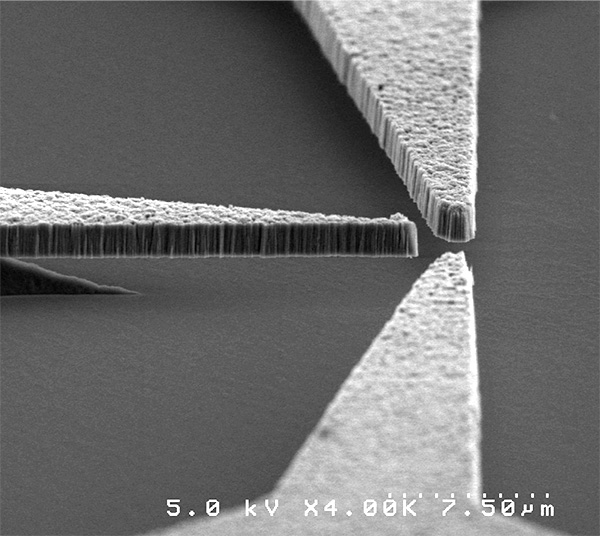
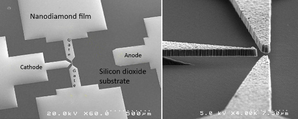 Left, electron micrograph of a nanodiamond field emission device. Right, detail of the device, showing the nanodiamond field emitter cantilevered above the insulating silicon dioxide surface. The silicon dioxide layer is on a silicon wafer. (Images, Davidson Lab, Vanderbilt University).[3]
The diamond devices are operable from liquid nitrogen temperature (77 K) all the way to about 500°C. They would also be inherently radiation resistant, so they would be useful in satellites and spacecraft. Two problems with this architecture are the definition of the gate, and the fact that some current is drawn through the gate.
Scientists from the NASA Ames Research Center (Moffett Field, CA) developed a planar process electron emission device in 2012 that they call a "vacuum channel transistor."[6] They built on previous work by the National Nanofab Center (Daejeon, Korea).[7-8] The device, as shown in the figure, uses a vertical architecture like the geometry of a standard MOSFET.
Left, electron micrograph of a nanodiamond field emission device. Right, detail of the device, showing the nanodiamond field emitter cantilevered above the insulating silicon dioxide surface. The silicon dioxide layer is on a silicon wafer. (Images, Davidson Lab, Vanderbilt University).[3]
The diamond devices are operable from liquid nitrogen temperature (77 K) all the way to about 500°C. They would also be inherently radiation resistant, so they would be useful in satellites and spacecraft. Two problems with this architecture are the definition of the gate, and the fact that some current is drawn through the gate.
Scientists from the NASA Ames Research Center (Moffett Field, CA) developed a planar process electron emission device in 2012 that they call a "vacuum channel transistor."[6] They built on previous work by the National Nanofab Center (Daejeon, Korea).[7-8] The device, as shown in the figure, uses a vertical architecture like the geometry of a standard MOSFET.
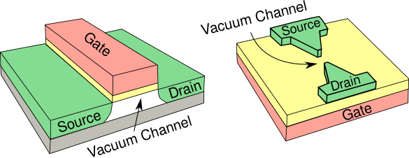 |
| The 2012 (left) and 2014 (right) versions of the NASA Ames Research Center vacuum channel transistor. (Illustration by the author using Inkscape.) |
References:
- C. A. Spindt, "A Thin‐Film Field‐Emission Cathode," Journal of Applied Physics, vol. 39, no. 7 (June 1, 1968), pp. 3504-3505.
- Charles A. Spindt, Kenneth R. Shouldersand Louis N. Heynick, "Field Emission Cathode Structures And Devices Utilizing Such Structures," US Patent No. 3,755,704, August 28, 1973.
- H. Dyball, "A diamond in the making," Electronics Letters, vol. 47, no. 16 (August 4, 2011), pp. 890ff., DOI:10.1049/el.2011.2314.
- David Salisbury, "Designing diamond circuits for extreme environments," Vanderbilt University Press Release, Aug. 4, 2011.
- L. Diederich, O.M. Küttel, P. Aebi and L. Schlapbach, "Electron affinity and work function of differently oriented and doped diamond surfaces determined by photoelectron spectroscopy," Surface Science, vol. 418, no. 1 (1998), pp. 219-239.
- Jin-Woo Han, Jae Sub Oh, and M. Meyyappan, "Vacuum nanoelectronics: Back to the future?—Gate insulated nanoscale vacuum channel transistor," Appl. Phys. Lett., vol 100, no. 21 (May 21, 2012), Document No. 213505, DOI: 10.1063/1.4717751.
- Gyu Hyeong Cho, Ji Yeoul Ryoo, Myeoung Wun Hwang, Min Hyung Cho, Young Jin Woo and Young Ki Kim, "Vacuum Field Transistor," US Patent No. 6,437,360, August 20, 2002.
- Dae Yong Kim and Hyun Tak Kim, "Vacuum Channel Transistor and Manufacturing Method thereof," US Patent No. 8,159,119, April 17, 2012.
- Jin-Woo Han and Meyya Meyyappan, "Introducing the Vacuum Transistor: A Device Made of Nothing," IEEE Spectrum, June 23, 2014.
- Peter Bright, "NASA melds vacuum tube tech with silicon to fill the terahertz gap," Ars Technica, June 24, 2014.
- Charles A. Spindt, Kenneth R. Shouldersand Louis N. Heynick, "Field Emission Cathode Structures And Devices Utilizing Such Structures," US Patent No. 3,755,704, August 28, 1973.