Metal-Air Transistor
February 4, 2019
I saw my first
atom on a
field trip to a
laboratory at
Le Moyne College,
Syracuse, NY. The laboratory did
research in
field ion microscopy.[1] As I wrote in an
earlier article (Imaging Atoms, September 26, 2012) and an article in a general interest
magazine,[2] When
scientists talk about "seeing" atoms, they just mean that they've seen some representation of them on an
imaging screen.
Sight involves sensing
reflected light from an object with our
eyes, sometimes with this light being
magnified in an
optical microscope. I didn't really see any atoms, since there was no direct linkage to the
human sense of sight.
The
Belgian surrealist artist,
René Magritte summarized this
idea in his
oil painting,
The Treachery of Images (La trahison des images, 1928–1929), in which he painted an
image of a
smoker's pipe with the
caption, "Ceci n'est pas une pipe" ("This is not a pipe"). Magritte's painting is an image of a pipe, and not a pipe.
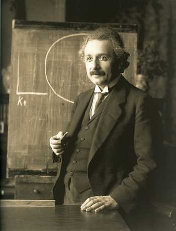
This is not Albert Einstein. Rather, it's a very nice image of Albert Einstein during a lecture in Vienna in 1921.
I would have shown René Magritte's The Treachery of Images (La trahison des images), but this is a copyrighted work of art.
You can view a low resolution image of his painting at Wikipedia.
(A 1921 photograph of Einstein by Ferdinand Schmutzer (1870-1928), as restored by Adam Cuerden, via Wikimedia Commons)
Field ion microscopy images the atoms of sharp
metal tips of less than about 50
nanometer tip
radius in a
vacuum chamber backfilled with an imaging
gas such as
helium,
argon, or
neon. Preparing these sharp tips is an art in itself that involves
etching and
electropolishing in an
electrolyte. Application of a high
positive voltage of the order of that used in a
cathode ray tube (5-10
kilovolts) with respect to the
phosphor screen will
ionize atoms of the imaging gas close to the tip. These positively-charged ions are repelled by the positively-charged tip in a direction
perpendicular to the
surface of the tip, and they will form a
magnified image of the tip on the phosphor screen.
Since a metal tip is an
electrical conductor, its surface is at a constant
electrical potential and the electric
field lines must be perpendicular at every surface
point. Since the tip is very sharp, the electric field lines have a large
angular divergence and there will be a large
field gradient at the sharp tip. Field ion imaging is enabled by this intense electric field gradient, which
accelerates the ions in
straight paths away from the tip.
Physicists are often criticized for their
"spherical cow" models, but there's a very instructive model that uses
spheres to
approximate the
geometry of a sharp tip to explain
electric charge bunching at the tip (see figure).[3]
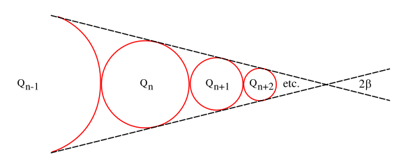
Sphere model for electric charge bunching at a sharp tip with a radius angle β. According to ref. 3, if the radii of successive spheres decrease by a constant factor k, we can calculate the angle of the tip radius, β = arcsin[(l-k)/(l+k)]. Setting a constant, γ = -ln(2)/ln(k), allows a calculation of the charge contained at the tip, σtip ∝ rtipγ, where rtip is the radius of the smallest sphere. (Created using Inkscape from data in ref. 3.[3])
While such imaging uses field emission of ions, emission of
electrons allows the creation of useful
devices, such as the
vacuum tube, a
component that defined
electronics through the
1950s. In vacuum tubes, electrons are emitted from a
heated cathode by
thermionic emission, but thermionic emission isn't the only way to generate an
electron beam.
Field emission of electrons will also happen at a sharp tip held at a high electrical potential according to the
Fowler–Nordheim equations. This effect was used by
Charles Spindt and his
colleagues at the
Stanford Research Institute (Menlo Park, California) in the
1970s, to make a
miniaturized field emission version of a vacuum tube.[4-5]
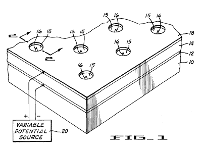
Fig. 1 of US Patent No. 3,755,704, "Field Emission Cathode Structures And Devices Utilizing Such Structures," by Charles A. Spindt, Kenneth R. Shouldersand Louis N. Heynick, August 28, 1973.
(Via Google Patents).[5]
![]()
A few improvements have been made to Spindt's concept since the 1970s. In 2011, a
research team from
Vanderbilt University made a field emission device from
diamond, a
material with an extremely low
work function, so it will produce field emission electron beams at low
voltage.[6-7] The properties of planar field emission devices are so similar to those of
transistors that many such devices are being called vacuum transistors, an example shown in the following figure.[8]
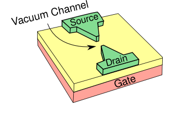
A vacuum channel transistor created by the NASA Ames Research Center (Moffett Field, CA).
The spacing between the electron emitter and collector can be made as small as 150 nm, which allows operation at less than 10 volts. This spacing is so much smaller than the mean free path of electrons in air that this vacuum transistor doesn't really need a vacuum.[8]
(Illustration by the author using Inkscape.)
The
Functional Materials and Microsystems Research Group of
RMIT University (Melbourne, Australia) have used the concept that electrons will easily transit a gap between
electrodes in air when the gap is very small to make a field emission air channel transistor (ACT).[9-11] Operation in air is possible since there is little likelihood that the emitted electrons will collide with an air
molecule. The
mean free path of the electrons is much larger than the gap.
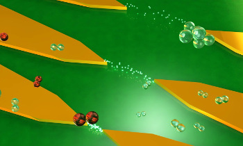
Artist's conception of electron transport in air channel transistors (ACTs).
The electron transport between electrodes is generally unimpeded by occasional gas molecules present in air.
RMIT University, Melbourne, Australia, image.
One motivation for this
research is the idea that we're reaching the limits of
Moore's Law, the idea that the number of transistors on a chip doubles every two years, with conventional
semiconductor transistors.[10] It's predicted that this doubling will end by the year 2025 when the dimensions of transistors can't decrease any further.[11] The
Australian research team believes that their ACT concept, which combines advanced
nanolithography with the vacuum tube principle, will extend Moore's Law by another two
decades.[9,11]
The exceptionally
low power and
high frequency operation of these ACTs arises from the unimpeded transport of electrons from one electrode to the other.[9-10] Electrons moving through a semiconductor will interact with its atoms, which slows their travel and produces
heat from
energy loss.[10] These devices are fabricated with
electron beam lithography, and this allows a gap spacing of less than 35 nm between
tungsten,
gold, or
platinum electrodes.[9] There's a bottom metal
gate to control the field emission, and the ACT devices can be fabricated on any
dielectric surface, as long as the this dielectric allows penetration of the bottom-gate field.[11]
Since the source and drain electrodes are
symmetric, the ACTs are bidirectional. They operate at voltages ≤2 volts at
currents in the tens of
nanoamperes range.[9] With tungsten and gold electrodes, the limiting process is Fowler–Nordheim
tunneling, while platinum electrodes exhibit
Schottky emission.[9] The
theoretical frequency limit for ACT devices is in the
terahertz range, which is 10 thousand times as fast as semiconductor devices.[11] One problem is that the metal tips of the electrodes experience localized
melting from the high electric field strength. This blunts the tips and reduces the emission
efficiency.[11]
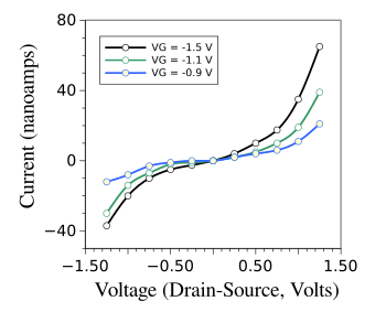
Current-voltage (I-V) curves at various gate voltages for an air channel transistor.
(Created with Gnumeric from data in ref. 9).[9]
![]()
Another advantage of ACTs over conventional transistors is that their fabrication is essentially a single-step process of
depositing the emitter (source) and collector (drain) electrodes spaced by the required air gap. The complex semiconductor transistor fabrication steps of
doping,
thermal processing,
oxidation, and
silicide formation are unnecessary.[11] As
Shruti Nirantar, a
Ph.D. candidate at RMIT and an
author of the
paper describing this research, remarks, "Devices can be built on ultrathin
glass,
plastics, and
elastomers... so they could be used in
flexible and
wearable technologies."[11] Just like vacuum tubes, the ACTs are
radiation resistant.[11]
References:
- C. C. Schubert, "Field‐ion microscopy in colour using multiple imaging gases," Journal of Microscopy, vol. 95, no. 3 (June, 1972), pp. 467-469, https://doi.org/10.1111/j.1365-2818.1972.tb01050.x.
- D.M. Gualtieri, Cyborgs and Atomic Microscopes, Phi Kappa Phi Forum, vol. 84, no. 2. pp. 6-7 (Spring 2004).
- H S Fricker, "Why does charge concentrate on points?" Phys. Educ., vol. 24 no. 3 (May 1989), pp. 157-161, https://doi.org/10.1088/0031-9120/24/3/309. Available as a PDF file here.
- C. A. Spindt, "A Thin‐Film Field‐Emission Cathode," Journal of Applied Physics, vol. 39, no. 7 (June 1, 1968), pp. 3504-3505.
- Charles A. Spindt, Kenneth R. Shouldersand Louis N. Heynick, "Field Emission Cathode Structures And Devices Utilizing Such Structures," US Patent No. 3,755,704, August 28, 1973.
LI> H. Dyball, "A diamond in the making," Electronics Letters, vol. 47, no. 16 (August 4, 2011), pp. 890ff., DOI:10.1049/el.2011.2314.
- David Salisbury, "Designing diamond circuits for extreme environments," Vanderbilt University Press Release, Aug. 4, 2011
- L. Diederich, O.M. Küttel, P. Aebi and L. Schlapbach, "Electron affinity and work function of differently oriented and doped diamond surfaces determined by photoelectron spectroscopy," Surface Science, vol. 418, no. 1 (1998), pp. 219-239
- Jin-Woo Han and Meyya Meyyappan, "Introducing the Vacuum Transistor: A Device Made of Nothing," IEEE Spectrum, June 23, 2014.
- Shruti Nirantar, Taimur Ahmed, Guanghui Ren, Philipp Gutruf, Chenglong Xu, Madhu Bhaskaran, Sumeet Walia, and Sharath Sriram, "Metal–Air Transistors: Semiconductor-Free Field-Emission Air-Channel Nanoelectronics," Nano Letters, Article ASAP (November 16, 2018), DOI: 10.1021/acs.nanolett.8b02849. A PDF file of supporting information is available here.
- Michael Quin, "Solution for next generation nanochips comes out of thin air," RMIT Press Release, November 20, 2018.
- John Boyd, "New Metal-Air Transistor Replaces Semiconductors," IEEE Spectrum, November 30, 2018.
Linked Keywords: Atom; field trip; laboratory; Le Moyne College; Syracuse, NY; research; field ion microscope; field ion microscopy; magazine; scientist; computer monitor; imaging screen; sight; reflection; reflected; light; eye; magnification; magnify; optical microscope; human sense; Belgian; surrealism; surrealist artist; René Magritte; idea; oil painting; The Treachery of Images (La trahison des images, 1928–1929); image; smoking pipe (tobacco); smoker's pipe; caption; Albert Einstein; lecture; Vienna; copyright; copyrighted; low resolution; Wikipedia; digital photography; photograph; Ferdinand Schmutzer (1870-1928); Adam Cuerden; Wikimedia Commons; metal; nanometer; radius; vacuum chamber; gas; helium; argon; neon; etching; electropolishing; electrolyte; electrical polarity; positive; voltage; cathode ray tube; kilovolt; phosphor; ionization; ionize; perpendicular; surface; magnification; magnify; electrical conductor; electrical potential; field line; point (geometry); angle; angular; divergence; electric field gradient; acceleration; accelerate; straight line; physicist; spherical cow model; sphere; approximation; approximate; geometry; electric charge; mathematical model; calculation; calculate; Inkscape; electron; electronic device; vacuum tube; electronic component; electronics; 1950s; electric heating; heated; hot cathode; thermionic emission; cathode ray; electron beam; Field emission of electrons; Fowler–Nordheim equations; Charles Spindt; colleague; Stanford Research Institute (Menlo Park, California); 1970s; field emitter array; miniaturized field emission version of a vacuum tube; Google Patents; research; Vanderbilt University; diamond; material; work function; voltage; transistors; vacuum; channel; field-effect transistor; NASA Ames Research Center (Moffett Field, CA); volt; mean free path; electron; atmosphere of Earth; air; Functional Materials and Microsystems Research Group; RMIT University (Melbourne, Australia); electrode; molecule; artist's impression; artist's conception; gas molecule; Moore's Law; semiconductor; Australia; Australian; nanolithography; decade; electric power; high frequency; heat; energy; electron beam lithography; tungsten; gold; platinum; gate; dielectric; symmetry; symmetric; electric current; nanoampere; quantum tunnelling; Schottky emission; theory; theoretical; terahertz; melting; efficiency; current-voltage (I-V) curve; Gnumeric; physical vapor deposition; deposit; doping (semiconductor); temperature; thermal; oxide; oxidation; silicide; Shruti Nirantar; Doctor of Philosophy; Ph.D.; author; scientific literature; paper; glass; plastic; elastomer; deflection; flexible; wearable technology; radiation hardening; radiation resistant.